Research Article Archive Versions 2 Vol 2 (2) : 19020202 2019
Download
EUV Lithography: State-of-the-Art Review
: 2019 - 05 - 10
: 2019 - 06 - 19
19306 1652 0
Abstract & Keywords
Abstract: Although several years delayed than its initial plan, extreme UV lithography (EUVL) with 13.5nm wavelength has been finally implemented into high volume manufacture (HVM) of mainstream semiconductor industry since 2018. With the delivery and installation of ASML EUV scanners in those giant Fab players like Samsung, TSMC and Intel, EUV lithography is becoming a sort of industry standard exposure metrology for those critical layers of advanced technology nodes beyond 7nm. Although ASML NXE EUVL scanner is the only commercialized EUV exposure system available on the market, its development is the concentration of all essence from worldwide industrial and academic collaboration. It is becoming more and more important not only for fab runners but also for main stream fabless design houses to understand and participate the progress of EUVL. In this review, working principles, module structures and technical challenges have been briefly discussed regarding each EUV subsystem, including light source, reflection mirrors and system, reticle module as well as photoresist development. EUV specific issues of light intensity, defectivity within reflection system, line edge roughness (LER) and mask 3D effects have been focused respectively and promising solutions have been summarized as well.
Keywords: EUV lithography; EUV review; mask 3D; line edge roughness; EUV light source
1.   Introduction
The development and growth of semiconductor industry has been following Moor’s low in recent 50 years, and it is fair to say that the continuous shrinking of transistors in microchips has been mainly driven by the development of photolithography technology[1,2,3]. Since the appearance of the first G-line (436nm wavelength) step-and-repeat system, namely wafer stepper, in late 1970s, this exposure system quickly has become mainstream and dramatically promoted the capability and efficiency of photolithography[4,5]. Due to the Rayleigh diffraction effect, smaller wavelength of light has to been adopted in order to get a reduced feature size with high resolution through a lens system, which makes a semiconductor device smaller. After jumping onto the fast lane of step-and-repeat system, the light source adopted in photolithography has been continuing switching from excimer laser for i-line (365nm)[6], to krypton fluoride (KrF) excimer laser for 248nm deep ultraviolet[7] and to argon fluoride (ArF) for 193nm wavelength in order to get even smaller feature size[8,9]. On this track, 157nm wavelength of F2 excimer laser was supposed to be produced to reach smaller half pitch than 65nm[10,11]. However, wavelength is not the only factor to improve the resolution of smaller pitches. Numerical aperture, NA as the Acronym, plays another role by the Rayleigh criterion:
R (smallest feature size) = k1 * λ / NA
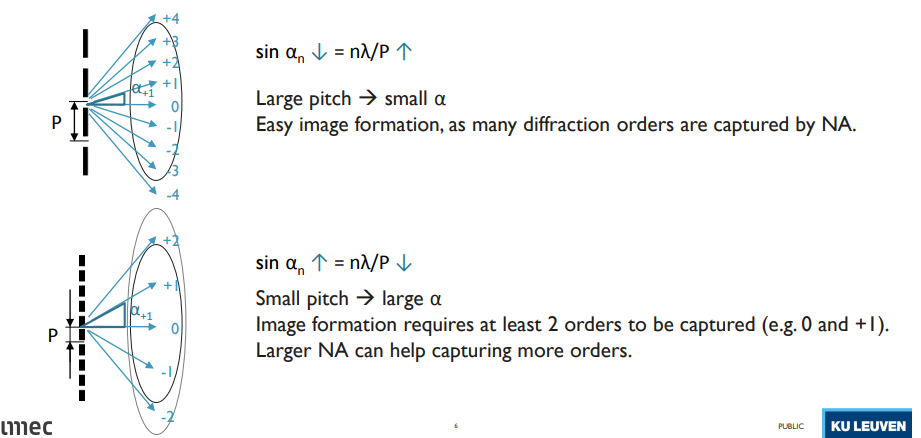
Where λ is the wavelength of the light used, NA is the numerical aperture of the system’s lens and k1 is known as the resolution factor and accounts for all other process variables. Furthermore, since NA=n*sinα, where α is the light incident angle and n is the refractive index of the medium surrounding the lens, and liquid has a larger n than air, an immersion ArF scanner was developed to reach a higher resolution for smaller features, in which immersion fluid (mainly water) is well controlled to stay between last lens and wafer surface in order to get higher NA[12] (Figure 1). The first commercial tool with this innovative technology was built and shipped by ASML in 2006 which started to dominate the market since then. The cost-effective implementation of immersion ArF scanner in the industry killed further development of tools with 157nm wavelength.


  Figure 1. Illustration of Rayleigh criterion. Larger NA benefits smaller pitches. Courtesy of Vu Luong, IMEC[14].
The implementation of immersion ArF scanner, enhanced by RET (Resolution Enhancement Technology) and multi-patterning technologies enabled the industry to reach 10nm/7nm FinFET tech node with acceptable cost, efficiency and die yield. But what is next? To resolve lines (half-pitch) smaller than 7nm, quadruple patterning or even more masks need to be used only for one functional layer, which will dramatically increase the cost and process variation. The industry has to follow Rayleigh criterion again to push the exposure wavelength to the limit.


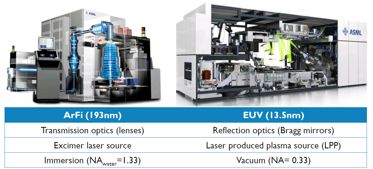
  Figure 2. Comparison of an ASML ArF immersion scanner and an ASML EUV scanner. Courtesy of Vu Luong, IMEC[14] .
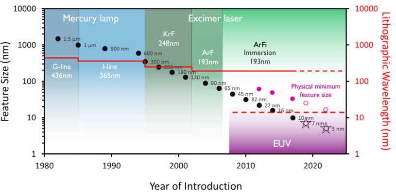
The industrialization of EUV lithography (EUVL) has been turned on since the turn of the 21st century and even earlier. Almost all key players from the industry and academic institutes have been involved in EUV light source development, Bragg mirrors with multi-coated layer, reflection system in vacuum, reflection reticle design and material development, EUV photoresist synthesis and optimization, contamination and defects reduction, DTCO (Design Technology Co-Optimization) and EDA tool development, as well as many other related engineering fields[13]. Most of the accomplishments of research and development have been concentrated to the ASML NXE EUVL module, which began its journey of High Volume Manufacture (HVM)[1,14] since 2017. Modern EUV scanner is equipped with a high power EUV light source which can generate 13.5nm wavelength radiation at a high power up to 250W (above 400W light source is also under development), a full refection mirror system in a vacuum chamber which prevent high adsorption on EUV optical path and maximize reflectivity, as well as redesigned reflection mirror and reticle system with 0.33 NA from Zeiss SMT to enable up to 140 wph (Wafer Per Hour) throughput. Figure 2 shows visual structures of a deep UV immersion module TWINSCAN NXT:1980i and a latest TWINSCAN NXE-3400B EUV module which is clearly distinguishable from the deep UV module due to the light reflection system. With the help of EUV lithography system, together with economic affordable multi-patterning technologies semiconductor technology node can be pushed further to beyond 3nm, and extend Moore’s Law to next decades (Figure 3). In the following chapter, main sub-modules of a EUV scanner will be briefly reviewed.


  Figure 3. Evolution of patterning resolution and lithographic wavelength. Courtesy of Vu Luong, IMEC[14].
2.   Light Source
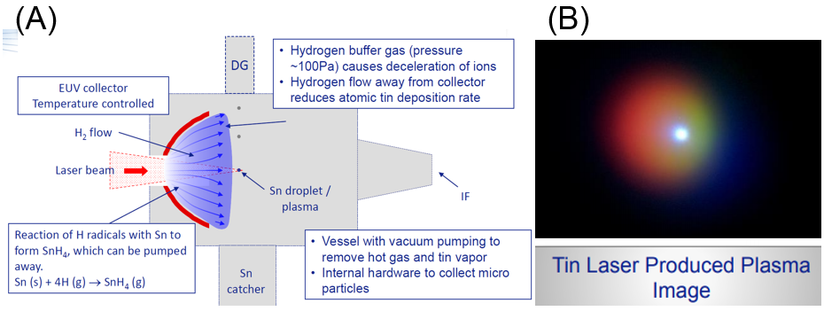
Unlike the direct deep UV generation from excimer lasers, extreme UV light with 13.5nm wavelength can only be produced by excitation and relaxation of relatively inner electrons of atoms (e.g. Sn20+), which could only be realized by atom ionization to form hot dense plasma[15,16,17]. In a commercial ASML EUV system, high power CO2 laser with 40~60kW has been applied to bombard liquid tin (Sn) droplet to generate dense plasma at high temperature around the droplet, where EUV radiation takes place[18,19]. EUV photons are collected by a multilayer coated collector in an ellipsoidal shape (Figure 4A) and conducted to the reflection optics in a scanner. As a standalone component of ASML EUV scanner, the LPP (laser produced plasma) EUV light source is composed of high power laser generator, laser beam delivery system and EUV source vessel, which is one of the most distinguish parts of a EUV system compared with deep UV scanners[15] . Due to the high gas absorption of 13.5nm wavelength UV light, the EUV vessel has to be kept in high vacuum which may suffer the system with particle contamination in contrast with deep UV chamber filled by clean nitrogen. In addition, high energy laser beam will evaporate liquid tin and produce tiny microparticles of tin vapor. These tin deposit contamination in the vacuum chamber was one of the biggest challenges in EUV system[20]. ASML is implementing hydrogen buffer gas with pressure about 100 Pa around the collector mirror to decelerate tin ions and reduce atomic tin deposition by a chemical reaction: Sn (s) + 4H (g) --> SnH4 (g), these SnH4 gas product can be pumped away from the chamber, as shown in Figure 4[21].


  Figure 4. (A) Illustration of EUV light source vessel with hydrogen gas as buffer. (B) An image of laser produced plasma around a tin droplet[21]. Courtesy of Igor Fomenkov, ASML
 
ASML subsidiary Cymer and Japan-based Company Gigaphoton are long-term rivals, both are struggling to win the battle to develop high power, high conversion efficiency light sources for EUV lithography applications[22].
The following paragraph describe main parts of a typical LPP system in a market-available ASML NXE 3x00 EUV system.
2.1.   CO2 Laser Generator and Power Amplifier
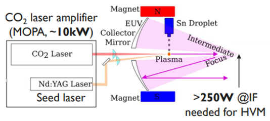
High power of input CO2 infrared laser is crucial to EUV final power output, which gives a second life of this mature laser technology[18,19] . It was proven that tin plasma EUV could be driven by CO2 laser pulse at 10.6 micron wavelength for the reasons of higher conversion efficiency, lower production of debris and higher average power levels without serious problems of beam distortions and nonlinear effects which occur normally in solid state lasers at high intensity. Practically a seed beam from Nd:YAG solid state laser at about 1 micron wavelength is preferred to be coupled together with the tin plasma as shown in Figure 5[14] . An optimal timescale for an energy coupling was found to be a few nanoseconds for the Nd:YAG lasers and around ten nanoseconds for the CO2 lasers.
The high power demand of a EUV source could be satisfied by a Master-Oscillator-Power-Amplifier system configuration. This new type of hybrid pulsed laser system combines pre-pulse seed laser, master oscillator, power amplifier (PA), fast flow systems, beam transport system and diffusion cooled planar waveguide lasers. The system can provide up to 40kW laser pulse, which could trigger 250W tin droplet EUV light source for latest ASML NXE 3400B EUV system with conversion efficiency (CE) up to 6%, so as to enable 140 wph (Wafer Per Hour) scanner throughput in HVM (High Volume Manufacturing)21. New generation of 60kW modern is under development in labs.


  Figure 5. Illustration of EUV generator. Incident CO2 and Nd:YAD laser beams hit tin droplet to generate dense plasma around the droplet, with the relaxation of plasma, EUV radiation takes place and focused by the collector mirror. Courtesy of Vu Luong, IMEC[14].
2.2.   Droplet Generator and Metrology
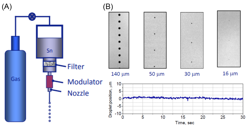
Inside the EUV source vessel, individual Sn droplets are continuously released with modulated size, speed and frequency from a nozzle of droplet generator (DG) located on top. As illustrated in Figure 6, tin raw material with high purity is melt in a container connected to the nozzle and pressed by an inert gas into the nozzle. Before spraying out of the nozzle, the tin jet is cut into droplets by mechanical vibration applied on in the nozzle under well-control. Separation space and size of droplets could be well-controlled by generator pressure and vibration frequency. Taking the nozzle outlet as a position reference, with the increasing distance from the outlet neighbor droplets coalesce together to from bigger droplets at larger separation space. The droplet size and timing must be precisely calculated and measured at the bombard position where laser pulse will hit the droplet to excite dense Sn+ plasma. This angry-bird-like process play a critical role in EUV light source generation, and it has been found the EUV power is proportional to droplets speed and space between droplets. All components must be modulated with highest precision.
ASML third generation droplet generator produces with 27µm diameter of droplet with about 2700 hours average lifetime[1] .


  Figure 6. (A) Illustration of Sn droplet generator. (B) Snapshot of Sn droplets with different size and interval. Courtesy of Vu Luong, IMEC[14].
2.3.   Multilayer Coated Collector
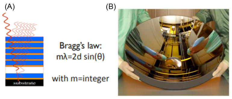
Plasma generated EUV light will be collected by an ellipsoidal MLM (Multi-Layer Mirror) collector with high reflectivity (Figure 7). The radius of the collector is well-designed to have its EUV focus on the vessel outlet called intermediate focus (IF) where EUV light is measured and conducted into the scanner vacuum chamber. In order to filter only 13.5nm EUV from the plasma halo and improve the reflective rate, collector surface is coated with multiple Mo/Si layers. By Bragg’s law n λ=2d*sin(θ), refection wavelength λ could be precisely selected by adjusting layer thickness d and refection angle θ. Main technical challenges include sputtering thickness and uniformity control of MLM layer, sputter target material purity, super fine polishing for surface roughness control, deposition of debris and contaminants, material decomposition and oxidation under EUV. The most advanced Bragg reflector of Mo/Si system can reach peak reflectance up to 70% (theoretically) of 13.5nm EUV light.


  Figure 7. (A) Illustration of multilayer coated on collector mirror[14]. (B) Photo of a real collector mirror from ASML[21]. Courtesy of Igor Fomenkov from ASML and Vu Luong from IMEC.
2.4.   System Power Efficiency
EUV light source power is critical for high volume manufacture. To get an acceptable throughput of over 100 wph, EUV source above 200W @ IF (Intermediate Focus) is needed. Key factors for high source power are high input CO2 laser power, high conversion efficiency (CE), high collection efficiency (reflectivity and lifetime) and advanced controls to minimize dose overhead, which follows below formula[1,23] :
EUV Power = (CO2 laser power * conversion efficiency [%]* transmission) * (1 – dose overhead [%])
Latest ASML NXE3400B system adopts a 40kW CO2 laser with system CE up to 6% and 10% dose overhead, which could generate 250W EUV light source. This enables wafer throughput up to 140 wph already acceptable for HVM. 400W EUV light source with 0.55 NA is under development at ASML, which will enable 185 wph throughput[1] .
3.   Reflection System and High NA
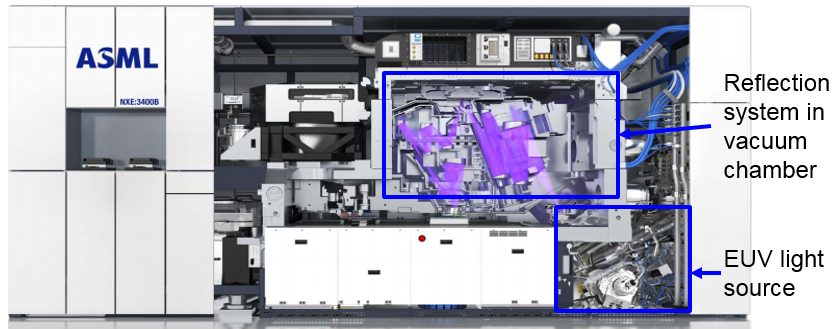
Due to the strong absorption of 13.5nm EUV to any gases, the whole optical path must be fully reflective and enclosed in a vacuum environment, which is different from that of a deep UV scanner system. Moreover, in order to further reduce absorption and boost reflectivity, metal-based reflection mirrors is coated with alternating molybdenum and silicon (MoSi) layers with several nanometer in thickness (called Bragg mirrors), similar as the collector in EUV light source vessel. High reflectance is achieved with careful control of mirror quality, layer thicknesses, multilayer materials, interface quality, and surface termination. After several years of research and development, reflectance and film properties are relatively stable and can satisfy the requirements of an advanced EUV lithography system. The reproducibility of the reflectance peak was characterized to be as small as 0.2 percent[24]. The coating uniformity has been improved to be better than 0.5 percent across a 150 mm diameter substrate[25].


  Figure 8. Internal structure of ASML NXE:3400B scanner. Source: ASML
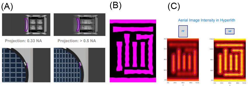
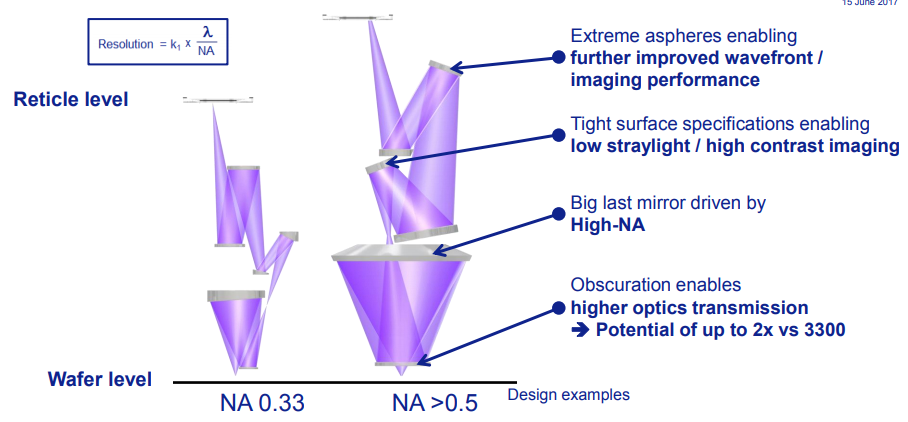
Reflection optics is also critical to next generation EUV scanner with high NA (> 0.5). High NA system will improve the wafer throughput to above 160 wph with dramatically reduced multi-pattern masks (number of LE), as shown in Figure 9. However, to reach high NA, reflection mirrors have to be redesigned to be asphere and the size of the mirror will be dramatically enlarged, accompany with EUV power over 400W[26]. Besides, anamorphic half filed reticle and exposure system has been introduced with 8x Y-magnification instead of traditional 4x magnification in both X and Y direction (Figure 9). Accordingly mask stage and wafer stage acceleration have to be adjusted to support twice number of scans/shots on wafer. Figure 10 illustrates mask comparison between 0.33 NA and 0.5 NA and wafer shot difference.


  Figure 9. (A) Anamorphic half field (HF) exposure with high NA compared with full field (FF) with 0.33 NA. (C) shows aerial image intensity mapping beteen FF and HF A from a test mask feature (B), where HF presents much higher contrast[28]. Courtesy of Jan van Schoot, ASML
High NA EUV will benefit wafer throughput and reduce mask layers, but at a cost of super high EUV light power, very large mirror, asymmetry and complicate reticle and wafer stage, as well as a special wafer cooling system. ASML future EXE module is supposed to be equipped with high NA optics[26,27,28] .


  Figure 10. EUV reflection comparison between NA=0.33 and high NA mirrors[26]. Courtesy of Anthony Yen, ASML
4.   EUV Mask
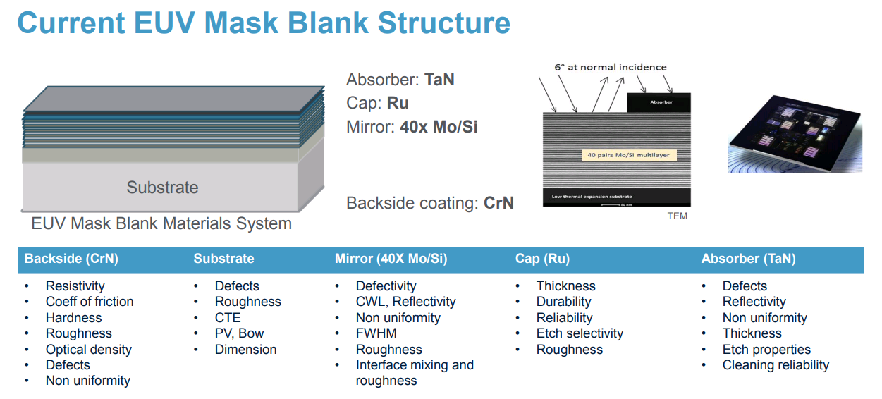
In the EUVL reflective optical system, a reflective reticle is crucial to imaging quality and lithography process window on wafer. Similar as multiple coating on reflective mirrors in the vacuum system, 40 pairs of Si/Mo layers are deposited on the substrate of an EUV mask in order to get maximum reflection, which are capped by a thin film of Ruthenium (Ru) as thermal emission and reinforcing layer[25,29]. On top of the thermal emission layer, absorber layers will be patterned to form “clear” or “dark” features. Material selection of absorber is critical to maximize absorption and minimize reflection. Shadowing effect and mask 3D effects are also related to absorber layer thickness and side-wall profile[30]. Moreover, UV, thermal and mechanical stability of the reticle also need to be considered.
4.1.   Pellicle Application
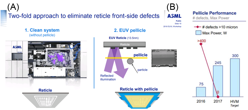
Usage of pellicle can prevent reticle from contamination and particles in the vacuum system, and greatly improve the lifetime of a reticle. But pellicle membranes on top of a reticle will reduce the EUV transmission and add extra cost to a reticle. ASML is struggling in both approaches: improve vacuum system cleanliness to avoid particle generation, and develop high performance pellicles membranes with high EUV transmission and low defect[28,26] . Progress has been made in recent years which makes the 1st generation pellicle ready for HVM which has been firmly tracked by Intel and other main EUV customers.
Advanced materials has been developed for pellicle membranes which should be durable under high power (> 300W) EUV radiation. SiNx is found to be a good backbone rigid materials for mechanical stability, Ru-capped SiN and Graphene sheet have been investigated at ASML and IBM, Graphite film is being developed at Samsung, Carbon Nanotube (CNTs) thin film composite with SiNx as a pellicle membrane has been developed and evaluated deeply at Hanyang University and IMEC. CNT enhanced SiNx membrane was found to have 2.5 times decrease of deflection when pressure applied, without scarify EUV transmission[31].


  Figure 11. (A) An ASML presentation slide illustrates pellicle application on an EUV reticle and how particle can be isolated from reticle surface by a pellicle. (B) Defects decreased with the application of pellicle[26]. Courtesy of Anthony Yen, ASML
4.2.   Mask Substrate and Bragg Mirror Layers
Physical properties of quartz glass based backbone influence aerial image deformation, and resist line edge roughness (LER) as well. Substrate macro properties like bow, material stress, surface roughness and flatness is determined by manufacturing process, e.g. lapping, cleaning, and fine CMP polishing. According to analysis from Applied Material, around 75% blank defects are introduced during manufacturing process of the substrate, compare to 25% of that from the deposition of multiple layers[25] . On the other hand, heat transmission and high temperature mechanical stability of materials are also concerned. Applied Materials has taken a lot of efforts on reticle blank material investigation and development and already made great progresses to improve substrate flatness, surface roughness, bow and defectivity to HVM level during last two years[25,29] .
Si/Mo switching Multilayers are sputtered on top of the substrate, which generate stress within multilayers and substrate interface as shown in Figure 12. One method is to selectively cut continuous mirror layer on uncritical area to release stress. Other critical properties which need to be preciously controlled are layer uniformity, thickness, interfacial roughness and defects within multilayers. It was observed that silicide formed within Si-Mo interface which could deteriorate EUV reflectivity, an optimized deposition process has been developed by Applied Materials to limit the silicide within sub-nm region, and such maximize reflectivity of EUV light[32].


  Figure 12. EUV reticle structure illustration from Applied Materials[29]. Courtesy of Vibhu Jindal, Applied Materials
 
A capping layer on top of mirror layer is needed to enhance mechanical durability and reliability of the reticle, and improve the adhesion between mirror layers and the absorber. Ruthenium was implemented as a capping layer in state-of-the-art EUV reticles, other advanced materials or composites have been investigated as well within major plays like Applied Materials and Veeco[33].
4.3.   Absorber and Mask 3D Effect
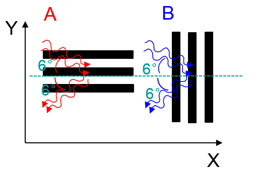
Mask 3D effect in EUVL is more predominant for wafer image quality, compared with that in DUV lithography. Thickness of absorber and Chief-ray Angle (CRA) introduce asymmetry EUV reflection, mask shadowing and different printing behavior between horizontal and vertical features, as shown in Figure 13 where horizontal patterns A suffers much higher shadowing effect than vertical pattern B due to off-axis incidence angle only in Y direction. Mask 3D effect is also a result of multilayer mirror reflectance changes over incidence and wavefront or phase deformation of the material. In current EUV scanner modules, horizontal and vertical lines show different CD variation and contrast[14] .
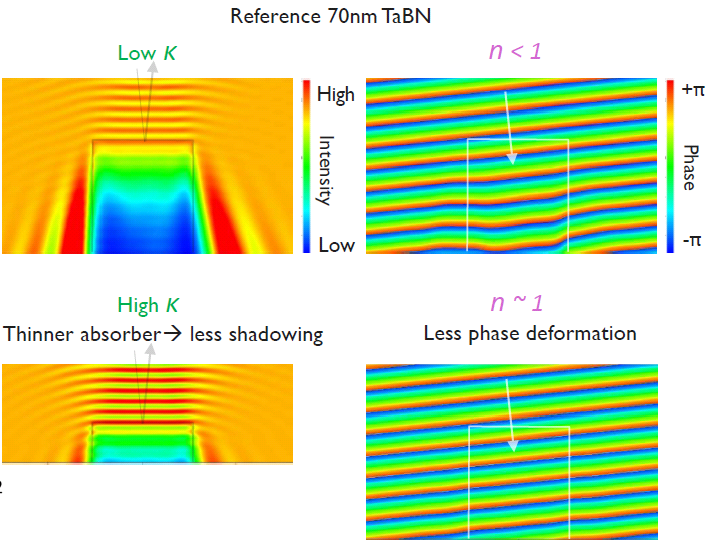
Ideal EUV absorber material should have a high extinction coefficient (k) and extremely low reflectivity, as well as small phase deformation after longtime EUV radiation at the same time, so that a reduced thickness and diminished 3D effect could be obtained. Boron doped TaN with about 70nm thickness is currently adopted for HVM EUV application with satisfactory results. But alternative absorber materials is also under evaluation. Today high-k absorbers such as Ni, Al, Co and their alloys have been evaluated by Veeco, IMEC[34], ASML together with mask shops like Toppan and Hoya[35], amorphous single phase materials as absorber is under development by Applied Materials[29] , which shows low surface roughness and stress, good chemical durability, good adhesion and etch selectivity with capping layer and less than 2% reflectivity for less than 45nm thickness. Pt-CrN Multilayer absorbers used for phase-shift mask (PSM) has been investigated by Hanyang University[36]. On the other hand, EDA vendor Synopsys has evaluated absorber side-wall angle impact on optical parameters like NILS and intensity latitude by simulation[30] .


  Figure 13. Feature orientation dependent mask 3D effect, horizontal features suffer more since they are perpendicular to the incident light plane.


  Figure 14. High k absorber can reduced mask 3D effect and get less phase deformation compared with low k absorber[14]. Courtesy of Vu Luong, IMEC
4.4.   Actinic Inspection and Defect of An EUV Mask
Mask defect is one of the major challenges limiting the high volume manufacture of EUVL system. Since EUV light will penetrate into multilayer structure on the mask and reflected back, both internal and surface defects have to be taken into account of amplitude and phase shift of the reflected EUV light. Each component of a mask multilayer can contribute to final defect formation. As mentioned in previous paragraph, the quality of a mask substrate is decided by its bow, surface flatness and roughness. Impurities or surface roughness can generate dislocations and lattice boundary on the substrate surface which can be easily extended to upper layers of the reticle and eventually reticle surface. Uniformity of the multilayer Bragg mirror may suffer from pits or bumps buried within 80x multilayers during sputtering deposition due to any contamination inside the chamber, gas or target impurities, thickness also vary on tool variation, so as the absorber, capping layers and pellicles. Contrary to deep UV masks, the surface roughness of an EUV mask causes phase variations of the incoming wave fronts, which lead to intensity variations in the aerial image i.e. speckles which are local intensity inhomogeneities[37,38]. Because of the reflective nature and much smaller wavelength, the speckles contrast is significantly higher than that of the deep UV masks and may increase Line Width Roughness (LWR) at wafer level.
Fortunately not all defects or impurities in multilayers (ML) will result in disaster of reticle scrap, some substrate defects can be de-magnified when they spread onto the reticle surface through ML of the mirror[39]. Some defects from multilayers can be locally repaired by E-beam similar as that for deep UV masks, as illustrated in Figure 15.
On the other hand, EUV mask characterization and actinic review of defects is also critical for HVM of EUVL since traditional SEM direct characterization cannot detect light phase changes and intensity variation due to mask internal defects or surface roughness. EUVL infrastructure consortium among ZEISS, SUNY Polytechnic Institute and SEMATECH has developed an actinic EUV mask Aerial Image Monitor System called AIMS™ EUV which is trying to close the gap[37] . With the help of AIMS system, aerial image of the mask could be obtained before wafer exposure, any phase changes or surface roughness from will be captured and their impact on wafer and line edge roughness will be evaluated automatically.


  Figure 15. Defect on EUV mask could be repaired. From left to right, it shows two dot defects on line-space features, defects removed, and an aerial image after reparation[37]. Courtesy of Dirk Hellweg, Zeiss SMT
5.   EUV Photo Resist
Stochastic effect of photo resist is another major concern for EUVL application[40,41,42]. Due to limited light source power, short wavelength and high photon energy of EUV light, Auger electrons or 2nd electrons will be generated after photon absorption by the resist, resulting in uncontrolled free electron path and photo acid spread after electronic relaxation, which is considered to be the main root cause of line edge roughness and CD variation[43,44]. Interdisciplinary teams worldwide have been working on understanding fundamental mechanism of photo chemical reaction, new material development, and process control.


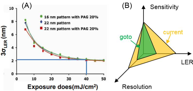
  Figure 16. (A) LER is strongly dependent on exposure dose. (B) Resist sensitivity, resolution and line edge roughness (LER) are correlated each other, an optimization of smaller LER with good resolution and sensitivity is needed for EUVL.
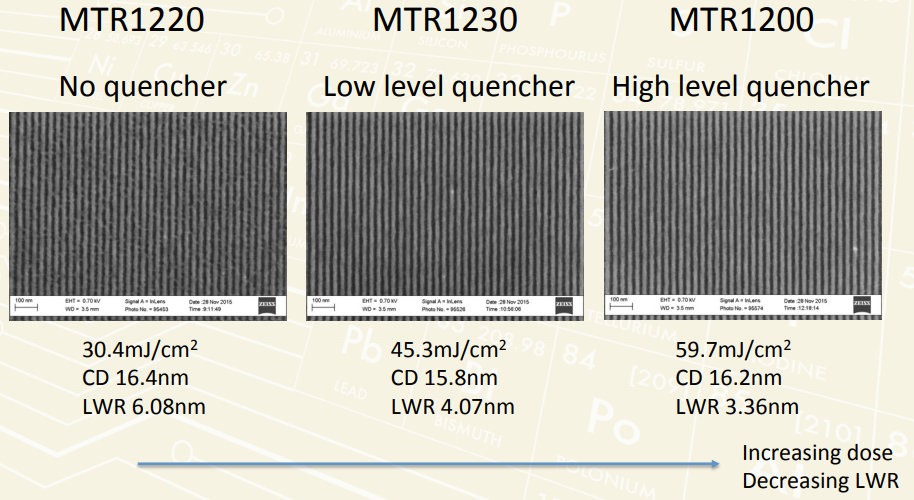
Gupta team from UCLA focus on LER analysis and impact on FEoL and BEoL of advanced FinFET technologies, LER mathematic model and LER impact on device reliability have been investigated[45]. Resist half-pitch (HP) resolution, dose sensitivity and their relationship (Figure 16) to LER have been evaluated by Paul Scherrer Institut (PSI) to get a comprehensive solution[46]. It was found that amount of photons, quencher and acid rank top three LER contributor, LER could be reduced by optimizing multi-trigger component ratio and quencher amount of the resist chemicals[47,48].
Metal-contained photoresist, chemical amplified resists (CARs), photo acids (PAs) together with their backbone polymers have been investigated, material quantum yield and absorption coefficient have been measured and correlated to electron mean free path within resist, providing a theoretical guide for photoresist selection. Resist chemical processes after EUV radiation are widely investigated by teams from Berkeley lab, Molecular Foundry, LBNL, Columbia Hill Technical Consulting and IBM Almaden Research Center[49,50]. Numeric model of imaging mechanism for sol-gel prepared organometallic polymer resists have been created by Inpria Corp., stochastic diffusion of secondary electrons has been simulated with changing dose[51]. Innovative Inorganic-organic composite photoresist with a metal oxide core and polymer ligands has been synthesized as a non-CAR resist which is supposed to have smaller LWR (3σ <3nm)[52,53,54]. Moreover, lithography process control and optimization are also essential to LER reduction. Toshiro Itani and Takahiro Kozawa from Japan have conducted experiments to improve line edge roughness by alternating development, bake, rinse solution as well as resist top and bottom coating[55].


  Figure 17. CDSEM images show LER is decreasing with increasing dose and resist quencher concentration[48]. Courtesy of C. Popescu, University of Birmingham
Outgassing is another issue during resist exposure, hydrogen-contained molecules can contaminate the vacuum chamber, mirrors and reticles. ASML has developed a Dynamic Gas Lock (DGL) membrane to prevent outgassing spread and suppress DUV and IR during the wafer exposure[1] .
6.   Summary and Outlook
In this paper, we had a broad but not specialized overview of extreme ultraviolet lithography technology and its application in mainstream semiconductor wafer manufacturing. Major EUVL modules include light source and vessel, reflection mirror system under vacuum, reflective reticle and aerial inspection system. Multilayer material fabrication and photoresist characterization are also critical in terms of EUV patterning performance, defectivity and edge roughness control. As EUVL scanner is an integrated system, final wafer printing quality is determined by every component especially the weakest ones. Thanks to worldwide collaboration and big investments in recent years, critical issues related to light source, substrate material and process, multilayer defects, mask absorber and defects, as well as resist edge roughness have been overcome in an ASML EUV scanner system, and wafer HVM using these EUV tools are already realized in those leading fabs worldwide.
Major progresses and challenges that are related to wafer throughput and pattern printing quality are summarized below.
EUV light source power
250W light power boosts wafer throughput to 140wph, which makes ASML EUV scanner ready for HMV. Next generation EUV source with further increased EUV energy power, improved conversion efficiency and better dose control is under development, not only to raise wafer throughput but also to further minimize LER which is closely related to dose on wafer. It was found 40mJ/cm2 dose (compared with 20mJ/cm2 from current module) can dramatically reduce LER to smaller than 3nm. 400W EUV source will be implemented in next module of ASML NXE scanner soon. High power EUV is also critical to next generation high NA scanner.
Mirror and reticle defectivity
Impurities, thickness inhomogeneity of multilayer mirrors and reticles can change EUV light intensity or phase which will generate defects on wafer. Reticle surface roughness also contributes to LER. Besides superb quality fabrication of multilayer mirrors and reticles, the control of contamination and particles in vacuum chamber is also a big concern since there is no clean pressure gap protection in the reflection chamber and high energy natural of EUV. With the introduction of pellicles and DGL membrane, chamber defects have been reduced to a very low level. In order to detect not only surface impurities but also light phase changes due to internal defects, AIMS inspection system has been developed by ZEISS together with SEMATECH. This tool could check wafer aerial image and detect potential pattern failure on wafer.
LER and CD variation
Compared with deep UV lithography, line edge roughness is much worse for EUVL due to relatively low dose and secondary electron diffusion (stochastic effect). New photo resists such as metal-oxide with polymer ligands are being developed, lithography process flow has been optimized, and reticle flatness is well-controlled, all efforts have successfully reduced the LER to an acceptable level for an ASML EUV system. Further investigation is trying to reduce LER to below 3nm for 3σ from current 3.5nm range from inorganic resist and 5nm range from CAR.
Mask 3D effect
Due to absorber thickness and the chief-ray angle of incident EUV light onto the mask, horizontal and vertical features show different imaging behavior and critical dimension change on wafer, this is called shadowing effect. Mask 3D is also related to reticle blank flatness and bow, multilayer EUV reflectivity, and absorber properties. These effects will decrease the margin of process window with a reduced or shifted depth of focus (DOF). By introducing phase control SMO and OPC correction, orientation-dependent mask CD bias could be compensated. High-k absorbers are also under development to help further reduce shadowing effect. In next generation of high-NA EUV scanner, anamorphic half filed reticle will be introduced to overcome x-y asymmetry and improve throughput[56], but with the cost of design, OPC and mask complexity.
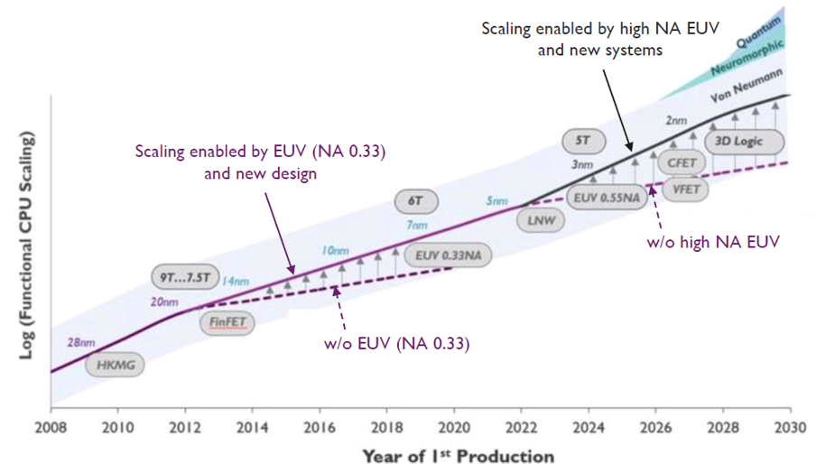
EUVL has achieved great progress since 2015, most of breakthroughs take place after the formation of EUV industry alliances among big player like ASML, INTEL, TSMC and SUMSANG. Industry requirements combined with strong financial support finally drive this technology into HVM. As the only EUVL scanner commercial provider, ASML is going to sell over 30 EUV modules in 2019. The market is ramping up and this revolutionary technology will lead the industry to the next decade[57] (Figure 18).


  Figure 18. Technology node scaling is driven by the development of lithography and DTCO. High NA EUV will lead the industry in next decade[14]. Courtesy of Vu Luong, IMEC

1 I. Fomenkov, “EUV Lithography : Progress in LPP Source Power Scaling and Availability”, 2017 International Workshop on EUV Lithography, Berkeley, CA, (2017).
2 Report from THE INTERNATIONAL ROADMAP FOR DEVICES AND SYSTEMS (IRDS): 2017, (2017).
3 P.Gargini, “Roadmap Evolution: From NTRS to ITRS, From ITRS 2.0 to IRDS”, Proc. SPIE 10450, (2017).
4 J. Mulkens et al, “High Throughput Wafer Steppers with Automatically Adjustable Conventional and
Annular Illumination Modes”, Proceedings of technical seminar: Semicon Japan, Ciba, (1995).
5 S. Wittekoek, “Optical Lithography: present status and contamination below 0.25 µm”, Microelectronic Engineering 23 , (1994).
6 B. Katz et al, “I-line Lithography for Sub Half Micron Design Rules” Proc. SPIE1927 , 298-310 (1993).
7 R. W. McCleary, P. J. Tompkins, M. D. Dunn, et al., "Performance of a KrF excimer laser stepper", Proc. SPIE 0922 , Optical/Laser Microlithography, (1988).
8 H. Kim, et al., “A novel platform for production-worthy ArF resist”, J. Photopolym. Sci. Tech.14 , 363, (2001).
9 Y. Trouiller, E. Luce, A. Barberet, et al., "Across field and across wafer flare: from KrF stepper to ArF scanner", Proc. SPIE 4000, Optical Microlithography XIII , (2000).
10 T. Ishimaru, S. Matsuura, M. Seki, et al., "Current status of 157-nm lithography using a full-field scanner", Proc. SPIE 5754, Optical Microlithography XVIII , (2005).
11 H. Nogawa, H. Hata, M. Kohno, "System design of a 157-nm scanner", Proc. SPIE 4691, Optical Microlithography XV , (2002).
12 S. Owa and H. Nagasaka "Immersion lithography; its potential performance and issues", Proc. SPIE 5040, Optical Microlithography XVI , (2003).
13 V. Bakshi, “EUV Lithography, Second Edition”, SPIE PRESS BOOK, (2018).
14 V. Luong, presentation “EUV Lithography Coming to your local IC manufacturer! SoonTM”, Arenberg Youngster Seminar, Leuven, (2018).
15 W. N. Partlo, D. J. W. Brown, I. V. Fomenkov, et al., “LPP EUV light source”, patent US7317196B2, United States.
16 A. I. Ershov, W. F. Marx, “Systems and methods for reducing the influence of plasma-generated debris on the internal components of an EUV light source”, patent US7196342B2, United States.
17 W. N. Partlo, N. Bowering, A. I. Ershov, et al., “EUV light source”, patent US7164144B2, United States.
18 K. M. Nowak, T. Ohta, T. Suganuma, et al., “CO2 laser drives extreme ultraviolet nano-lithography - second life of mature laser technology”, Opto-Electron. Rev.21 , no. 4, (2013).
19 T. Ariga, H. Hoshino, T. Miura et al., "High-power pulsed CO2 laser for EUV lithography", Proc. SPIE 6151 , Emerging Lithographic Technologies X, (2006).
20 A. I. Ershov, A. N. Bykanov, O. Khodykin, et al., “LPP EUV light source drive laser system”, patent US7439530B2, United States.
21 I. Fomenkov, presentation “EUV Source for High Volume Manufacturing: Performance at 250 W and Key Technologies for Power Scaling”, 2017 Source Workshop, Dublin, Ireland, (2017).
22 V. Banine, R. Moors, “Plasma sources for EUV lithography exposure tools”, J. Phys. D: Appl. Phys.37 , 3207, (2004).
23 V. Banine and R. Moors, “Plasma sources for EUV lithography exposure tools”, Journal of Physics D: Applied Physics37 , Number 23, (2004).
24 V. Jindal, G. Fong, S. Liu, et al., “Advanced deposition techniques for next generation EUV mask blanks”, EUVL Workshop 2018, Berkeley, CA (2018).
25 A. Rastegar, presentation “EUV Mask Substrate Readiness For Sub 10 nm HP Nodes”, EUVL Workshop 2018, Berkeley, CA (2018).
26 A. Yen, presentation “Continued Scaling in Semiconductor Manufacturing with EUV Lithography”, EUVL Workshop 2018, Berkeley, CA (2018).
27 J. van Schoot et al, presentation “EUV roadmap extension by higher Numerical Aperture”, EUVL conference 2016, Hiroshima, Japan (2016).
28 J. van Schoot, B. Kneer, et al, presentation “High-NA EUV lithography enabling Moore’s law in the next decade”, EUVL Workshop 2017, Berkeley, CA (2017).
29 V. Jindal, G. Fong, S. Liu, et al., presentation “Advanced deposition techniques for next generation EUV mask blanks”, EUVL Workshop 2018, Berkeley, CA (2018).
30 T. Fühner, L. S. Melvin III, Y. Kandel et al., presentation “EUVL mask engineering in the third dimension the impact of absorber sidewall angles on imaging behavior”, EUVL Workshop 2018, Berkeley, CA (2018).
31 S. J. Wi, Y. J. Jang, J. Ahn, presentation “Evaluating thermal and mechanical properties of composite films for EUV pellicle applications”, EUVL Workshop 2018, Berkeley, CA (2018).
32 S. Vernon, P. Kearney, W. Tong et al., “Masks for extreme ultraviolet lithography”, Proc. SPIE - The International Society for Optical Engineering10.1117 , 12.332826, (1998).
33 K. Rook, M. Lee, S. Kohli, A. Devasahayam, et al., presentation “High-volume manufacturing of EUV mask blanks status and roadmap”, EUVL Workshop 2018, Berkeley, CA (2018).
34 V. Luong, V. Philipsen, E. Hendrickx, et al., “Ni-Al alloys as alternative EUV mask absorber”, Appl. Sci.,8(4) , 521, (2018).
35 J. Finders, et al. “Experimental investigation of a high-k reticle absorber system for EUV lithography”, Extreme Ultraviolet (EUV) Lithography X, Conference 10957, (2019).
36 J. S. Kim, G. W. Dong, D. M. Jeong, “Fabrication and evaluation of phase shift mask using platinum for high numerical aperture extreme ultraviolet lithography”, Extreme Ultraviolet (EUV) Lithography X, Conference 10957, (2019).
37 D. Hellweg, M. Koch, S. Perlitz, et al., “Actinic review of EUV Masks: performance data and status of the AIMSTM EUV system”, Proc. SPIE10143 , 101430J (2017).
38 X. Chen, E. Verduijn, O. Wood, et al., “Evaluation of EUV mask impacts on wafer line-width roughness using aerial and SEM image analyses”, Extreme Ultraviolet (EUV) Lithography IX, SPIE 10583, (2018).
39 S. P. Vernon, P. A. Kearney, W. M. Tong, et al., “Masks for extreme ultraviolet lithography”, Proc. SPIE 3546 , 18th Annual BACUS Symposium on Photomask Technology and Management, (1998).
40 R. L. Brainard, P. Trefonas, J. H. Lammers, et al., "Shot noise, LER, and quantum efficiency of EUV photoresists", Emerging Lithographic Technologies VIII, Proc. SPIE 5374 , (2004).
41 P. De Bisschop "Stochastic effects in EUV lithography: random, local CD variability, and printing failures," Journal of Micro/Nanolithography, MEMS, and MOEMS 16(4), 041013, (2017).
42 P. De Bisschop, J. Van de Kerkhove, J. Mailfert, et al., "Impact of stochastic effects on EUV printability limits", Extreme Ultraviolet (EUV) Lithography V, Proc. SPIE 9048 , (2014).
43 Kim, Sang-Kon. "Modeling and simulation of line edge roughness for EUV resists." JSTS: Journal of Semiconductor Technology and Science14.1 , 61-69, (2014).
44 M. Nassir, J. Gobrecht, Y. Ekinci. "Beyond EUV lithography: a comparative study of efficient photoresists' performance." Scientific reports 5 , 9235, (2015).
45 Y. Luo, P. Gupta "Relaxing LER requirement in EUV lithography", Design-Process-Technology Co-optimization for Manufacturability XII, Proc. SPIE 10588 , (2018).
46 Y. Ekinci, presentation “Pushing the resolution limits of photolithography: Understanding the fundamentals of the EUV resists”, EUVL Workshop 2018, Berkeley, CA (2018).
47 P. Naulleau, “EUV lithography patterning challenges”, Materials and Processes for Next Generation Lithography, Elsevier, (2016).
48 C. Popescu, A. McClelland, J. Roth, et al., “MTR resist for reduced LER in EUV lithography”, EUVL Workshop 2018, Berkeley, CA (2018).
49 O. Kostko, B. Xu, M. Ahmed, et al., “Fundamental understanding of chemical processes in extreme ultraviolet resist materials”, J. Chem. Phys.149 , 154305, (2018).
50 A. Robinson, R. Lawson, “Materials and Processes for Next Generation Lithography”, Volume 11, Pages 1-608, Elsevier, (2016).
51 W. Hinsberg, S. Meyers, “A numeric model for the imaging mechanism of metal oxide EUV resists”, EUVL Workshop 2018, Berkeley, CA (2018).
52 S. Castellanos, “EUV resist: the great challenge of small things”, EUVL Workshop 2018, Berkeley, CA (2018).
53 O. Yildirim, E. Buitrago, R. Hoefnagels, et al., “Improvements in resist performance towards EUV HVM”, Extreme Ultraviolet (EUV) Lithography VIII, Proc. SPIE 10143 , (2017).
54 L. Li, X. Liu, S. Pal, et al., “Extreme ultraviolet resist materials for sub-7 nm patterning”, Chem Soc Rev., 46 (16), 4855-4866, (2017).
55 T. Itani, T. Kozawa, “Resist materials and processes for extreme ultraviolet lithography”, Japanese Journal of Applied Physics 52 , Number 1R, (2012).
56 V. Wiaux, V. Philipsen, E. Hendrickx, “Mask 3D effects first experimental measurements with NA 0.55 anamorphic imaging”, EUVL Workshop 2018, Berkeley, CA (2018).
57 R. Kim, Y. Sherazi, P. Debacker, et al., "IMEC N7, N5 and beyond: DTCO, STCO and EUV insertion strategy to maintain affordable scaling trend", Design-Process-Technology Co-optimization for Manufacturability XII, Proc. SPIE 10588, (2018).
Article and author information
Nan Fu
Yanxiang Liu
Xiaolong Ma
Zanfeng Chen
Publication records
Published: June 19, 2019 (Versions2
References
Journal of Microelectronic Manufacturing